4.3.1 Main circuit connection diagram
4.3.1.1 Main circuit connection diagram of VFDs of AC 3PH 380V (-15%)–440V (+10%)
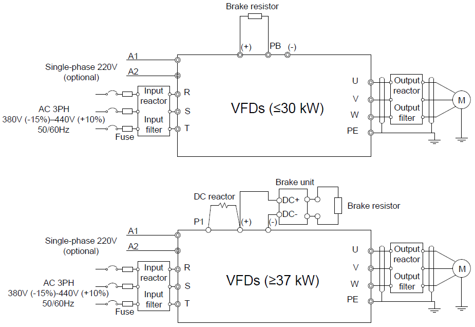
Figure 4-7 Main circuit connection diagram of 380V VFDs
Note:
The fuse, DC reactor, braking unit, braking resistor, input reactor, input filter, output reactor, output filter are optional parts. Please refer to Peripheral Optional Parts for detailed information.
A1 and A2 are optional parts.
P1 and (+) are short circuited in factory for the VFDs of 380V (≥37kW), if need to connect with the DC rector, please remove the contact tag between P1 and (+).
Before connecting the braking resistor cable, remove the yellow labels of PB, (+), and (-) from the terminal blocks. Otherwise, poor connection may occur.
4.3.1.2 Main circuit connection diagram of VFDs of 3PH 380V (-10%)–550V (+10%)
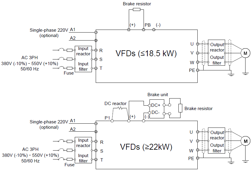
Figure 4-8 Connection diagram of main circuit for the VFDs of 500V
Note:
The fuse, DC reactor, braking unit, braking resistor, input reactor, input filter, output reactor, output filter are optional parts. Please refer to Peripheral Optional Parts for detailed information.
A1 and A2 are optional parts.
P1 and (+) are short circuited in factory for the VFDs of 500V (≥22kW), if need to connect with the DC rector, please remove the contact tag between P1 and (+).
Before connecting the braking resistor cable, remove the yellow labels of PB, (+), and (-) from the terminal blocks. Otherwise, poor connection may occur.
4.3.1.3 Main circuit connection diagram of VFDs of AC 3PH 520V (-15%)–690V (+10%)
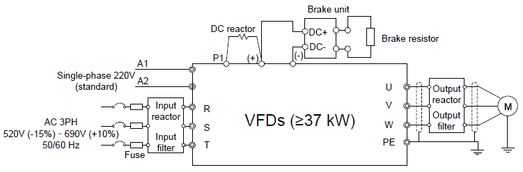
Figure 4-9 Connection diagram of main circuit for the VFDs of 660V
Note:
The fuse, DC reactor, braking unit, braking resistor, input reactor, input filter, output reactor, output filter are optional parts. Please refer to Peripheral Optional Parts for detailed information.
A1 and A2 are standard parts.
P1 and (+) are short circuited in factory, if it needs to connect with the DC rector, please remove the contact tag between P1 and (+).
Before connecting the braking resistor cable, remove the yellow labels of PB, (+), and (-) from the terminal blocks. Otherwise, poor connection may occur.
4.3.2 Main circuit terminals diagram
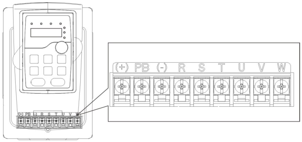
Figure 4-10 Main circuit terminals diagram of VFDs of 380V (1.5–2.2kW)
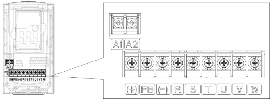
Figure 4-11 Main circuit terminals diagram of VFDs of 380V (4–5.5kW)
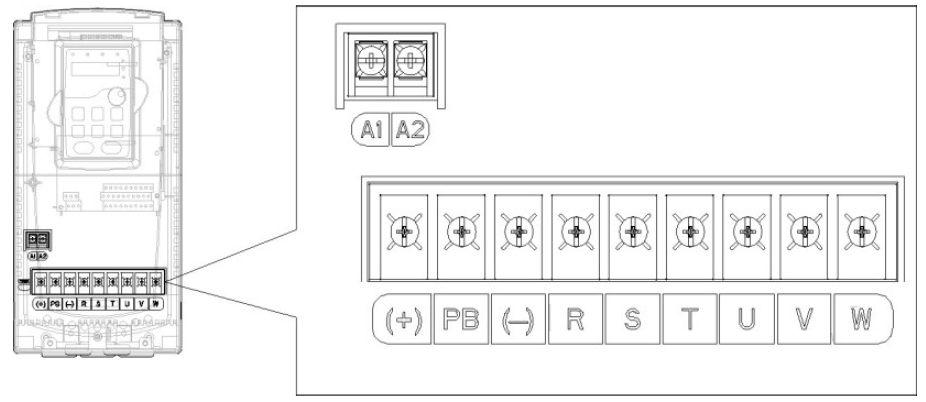
Figure 4-12 Main circuit terminals diagram of VFDs of 380V (7.5–11kW) and 500V (4–18.5kW)
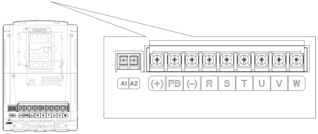
Figure 4-13 Main circuit terminals diagram of VFDs of 380V (15–18kW)
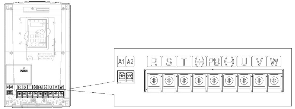
Figure 4-14 Main circuit terminals diagram of VFDs of 380V (22–30kW)
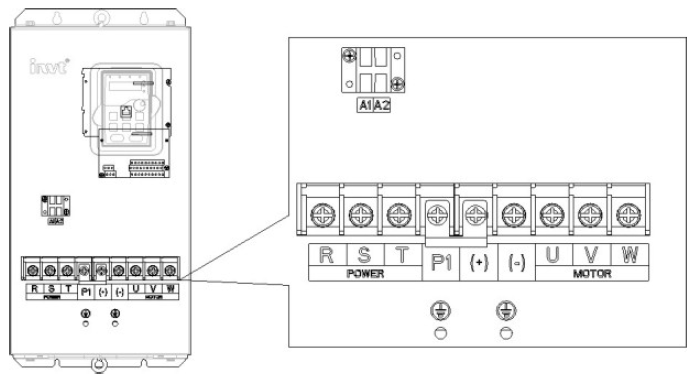
Figure 4-15 Main circuit terminals diagram of VFDs of 380V (37–55kW), 500V (22–55kW), and 660V (22–45kW)
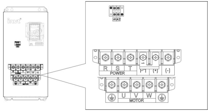
Figure 4-16 Main circuit terminals diagram of VFDs of 380V (75–110kW), 500V (75kW), and 660V (55–132kW)
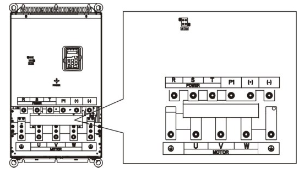
Figure 4-17 Main circuit terminals diagram of VFDs of 380V (132–200kW) and 660V (160–220kW)
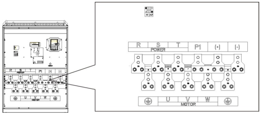
Figure 4-18 Main circuit terminals diagram of VFDs of 380V (220–315kW) and 660V (250–350kW)
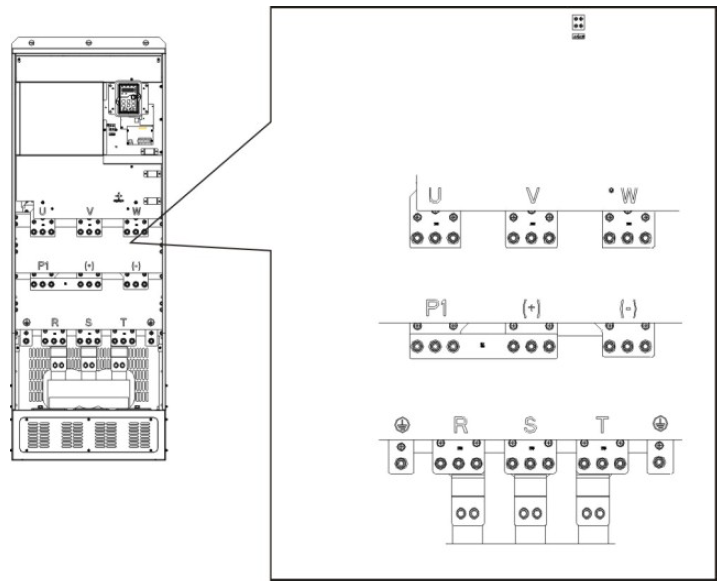
Figure 4-19 Main circuit terminals diagram of VFDs of 380V (350–500kW) and 660V (400–630kW)
Terminal | Terminal name | Function description | ||
380V (≤30kW) | 380V (≥37kW) | |||
500V (≤18.5kW) | 500V (≥22kW) | |||
660V | ||||
R,S,T | Power input of the main circuit | 3-phase AC input terminals which are generally connected with the power supply. | ||
U,V,W | VFD output | 3-phase AC output terminals which are generally connected with the motor. | ||
P1 | / | DC reactor terminal 1 | P1 and (+) are connected with the terminals of the DC reactor. (+) and (-) are connected with the terminals of the braking unit. PB and (+) are connected with the terminals of the braking resistor. | |
(+) | Braking resistor 1 | DC reactor terminal 2, braking unit terminal 1 | ||
(-) | / | Braking unit terminal 2 | ||
PB | Braking resistor 2 | / | ||
PE | 380V/500V/660V: the grounding resistor is less than 10 Ohm
| Protective grounding terminals. Every machine is provided with 2 PE terminals as the standard configuration. These terminals must be grounded with proper techniques. | ||
A1 and A2 | Control power supply terminal | Optional parts for 380V VFDs, standard parts for 660V VFDs (connected with external 220V control power supply), enabling a VFD to use an auxiliary power supply when no power is applied in the input main circuit, thus facilitating the commissioning of the VFD and improving safety during the commissioning. | ||
Note:
Do not use an asymmetrically constructed motor cable. If there is a symmetrically constructed grounding conductor in the motor cable in addition to the conductive shield, connect the grounding conductor to the grounding terminal at the VFD and motor ends.
Braking resistor, braking unit and DC reactor are optional parts.
Route the motor cable, input power cable and control cables separately.
If the terminal description is "/", the machine does not provide the terminal as the external terminal.
4.3.3 Main circuit terminal wiring
1. Connect the ground line of input power cable to the ground terminal of VFD (PE) directly, and connect 3PH input cable to R, S and T and fasten up.
2. Connect the ground line of motor cable to the ground terminal of the VFD, and connect the 3PH motor cable to U, V, W and fasten up.
3. Connect the brake resistor which carries cables to the designated position.
4. Fasten up all the cables on the outside of the VFD if allowed.
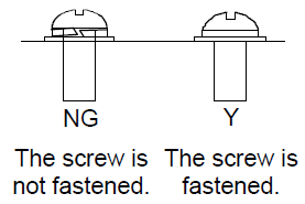
Figure 4-20 Correct installation of the screw
4.3.4 Control circuit wiring diagram
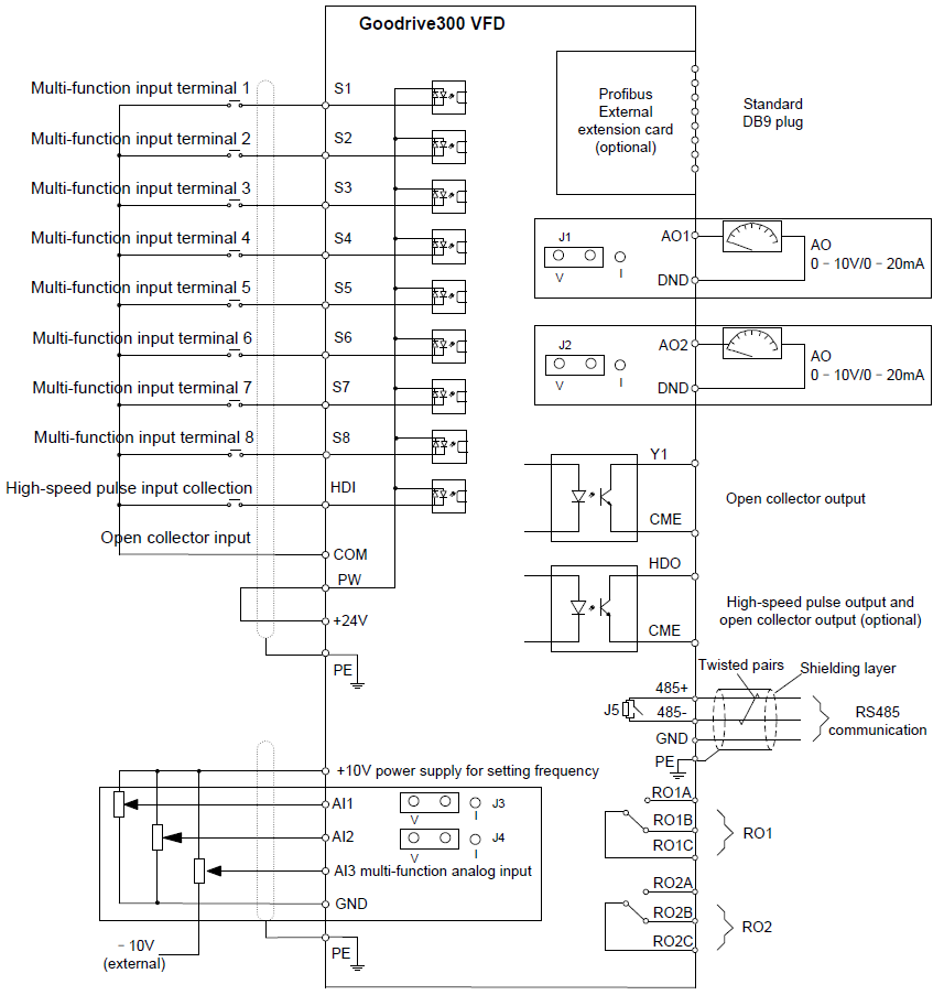
Figure 4-21 Control circuit wiring
4.3.5 Control circuit terminal diagram
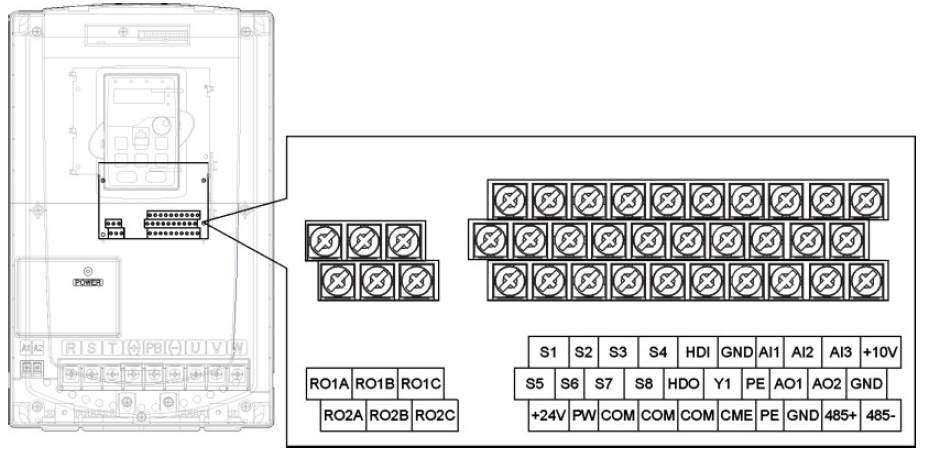
Figure 4-22 Control circuit terminals
Terminal name | Description | ||||
+10V | Local power supply +10 V | ||||
AI1 | 1. Input range: AI1/AI2 voltage and current can be chosen: 0–10 V/0–20mA; AI1 can be shifted by J3 while AI2 can be shifted by J4; AI3: -10 V–+10 V 2. Input impedance: voltage input: 20kΩ; current input: 500Ω 3. Resolution: the minimum one is 5m V when 10 V corresponds to 50 Hz 4. Deviation ±1%, 25°C | ||||
AI2 | |||||
AI3 | |||||
GND | +10 V reference null potential | ||||
AO1 | 1. Output range: 0–10 V or 0–20mA; The voltage or the current output is depended on the jumper. AO1 is switched by J1 and AO2 is switched by J2 2. Deviation±1%, 25°C | ||||
AO2 | |||||
Terminal name | Description | |||
RO1A | RO1 relay output; RO1A is NO, RO1B is NC, RO1C is common port Contact capacity: 3A/AC250V, 1A/DC30V | |||
RO1B | ||||
RO1C | ||||
RO2A | RO2 relay output; RO2A is NO, RO2B is NC, RO2C is common port Contact capacity: 3A/AC250V, 1A/DC30V | |||
RO2B | ||||
RO2C | ||||
Terminal name | Description | |||
HDO | 1. Switch capacity: 200mA/30V; 2. Range of output frequency: 0–50kHz | |||
COM | Common port of +24V | |||
CME | Common port of open collector output | |||
Y | 1. Switch capacity: 200mA/30V; 2. Range of output frequency: 0–1kHz | |||
485+ | For 485 communication port, 485 differential signal port and standard 485 communication interfaces, use twisted pairs or shielded cables. | |||
485- | ||||
Terminal name | Description | |||||||
PE | Grounding terminal | |||||||
| PW | Provide input digital working power from external to internal; Voltage range: 12–30V. | ||||||
24V | The VFD provides user power; the maximum output current is 200mA | |||||||
COM | Common port of +24V | |||||||
S1 | Digital input 1 | 1. Internal impedance: 3.3kΩ 2. Accept 12–30V voltage input 3. This terminal is bi-directional input terminal and supports NPN/PNP connection modes 4. Max. input frequency: 1kHz 5. All are programmable digital input terminals, and users can set the terminal function via function codes | ||||||
S2 | Digital input 2 | |||||||
S3 | Digital input 3 | |||||||
S4 | Digital input 4 | |||||||
S5 | Digital input 5 | |||||||
S6 | Digital input 6 | |||||||
S7 | Digital input 7 | |||||||
S8 | Digital input 8 | |||||||
HDI | Besides S1–S8 functions, it can also act as high frequency pulse input channel Max. input frequency: 50kHz | |||||||
4.3.6 Input /Output signal connection figure
Use U-shaped short-circuit connectors to set NPN mode or PNP mode and the internal or external power supply. The default setting is NPN internal mode.

Figure 4-23 U-shaped short-circuit positions
If the signal is from NPN transistor, set the U-shaped short-circuit connector between +24V and PW as follows according to the used power supply.
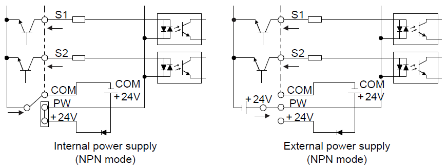
Figure 4-24 NPN modes
If the signal is from PNP transistor, set the U-shaped short-circuit connector as follows according to the used power supply.
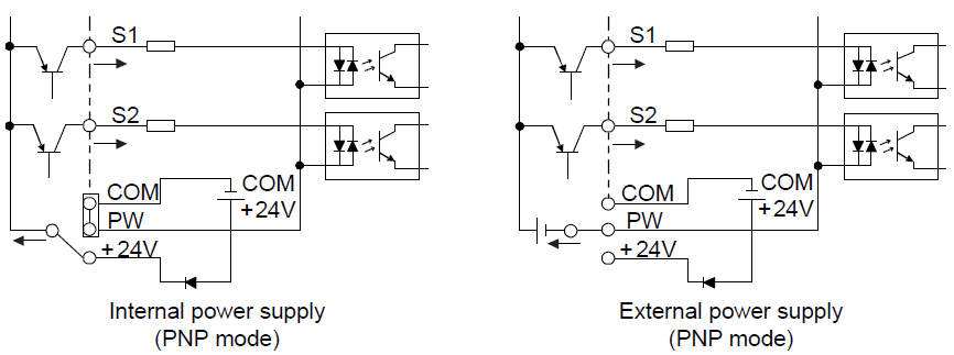
Figure 4-25 PNP modes