4.4.1 Basic control circuit wiring diagram
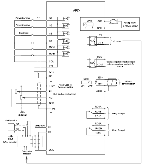
Figure 4.15 Control circuit wiring diagram
Terminal name | Description | |
+10V | Locally provided +10.5V power supply | |
AI1 | l Input range: AI1 voltage/current can choose 0–10V / 0–20mA; AI2: -10V – +10V; l Input impedance: 20kΩ during voltage input; 250Ω during current input; l Whether the input is voltage or current is set through P05.50; l Resolution ratio: When 10V corresponds to 50Hz, the min. resolution ratio is 5mV; l Deviation: ±0.5% at 25°C, when input is above 5V/10mA. | |
AI2 | ||
GND | +10.5V reference zero potential | |
AO1 | l Output range: 0–10V or 0–20mA l Whether the output is voltage or current is set through the switch SW2 l Deviation: ±0.5% at 25°C, when input is above 5V/10mA. | |
RO1A | l RO1 relay output; RO1A is NO, RO1B is NC, RO1C is common terminal l Contact capacity: 3A/AC250V, 1A/DC30V | |
RO1B | ||
RO1C | ||
RO2A | l RO2 relay output; RO2A is NO, RO2B is NC, RO2C is common terminal l Contact capacity: 3A/AC250V, 1A/DC30V | |
RO2B | ||
RO2C | ||
HDO | l Switch capacity: 50mA/30V l Range of output frequency: 0–50kHz l Duty ratio: 50% | |
COM | Common terminal of +24V | |
CME | Common terminal of open collector output; short connected to COM by default | |
Y1 | Switch capacity: 50mA/30V Range of output frequency: 0–1kHz | |
485+ | RS485 communication port, RS485 differential signal port and standard RS485 communication port must use twisted shielded pair; the 120ohm terminal matching resistor of RS485 communication is connected by the switch SW3. | |
485- | ||
PE | Grounding terminal | |
PW | Used to provide input digital working power from the external to the internal. Voltage range: 12–30V | |
24V | User power provided by the VFD, maximum output current 200mA. | |
COM | Common terminal of +24V | |
S1 | Digital input 1 | l Internal impedance: 3.3kΩ l Accept 12–30V voltage input l Bi-directional input terminal, supporting NPN/PNP connection modes l Max. input frequency: 1kHz l All are programmable digital input terminals, the functions of which be set through function codes |
S2 | Digital input 2 | |
S3 | Digital input 3 | |
S4 | Digital input 4 | |
HDIA | l Besides S1–S4 functions, the terminals can also act as high frequency pulse input channels l Max. input frequency: 50kHz; l Duty ratio: 30%–70%; l Supporting 24V-power quadrature encoder input; equipped with speed-measurement function | |
HDIB | ||
+24V—H1 | STO input 1 | l Safe torque off (STO) redundant input, connected to the external NC contact. When the contact opens, STO acts and the VFD stops output; l Safety input signal wires use shielded wires whose length is within 25m; l The H1 and H2 terminals are short connected to +24V by default. Remove the short connectors from the terminals before using STO function. |
+24V—H2 | STO input 2 | |
4.4.2 Input/output signal connection diagram
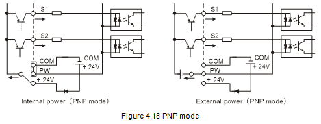
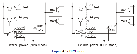
You can select the NPN/PNP mode and internal/external power through the U-type short connector. NPN internal mode is adopted by default.
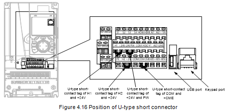
Note: The USB port can be used to upgrade the software, and the keypad port can be used to connect an external keypad. The external keypad cannot be used when the keypad of the VFD is used.
If input signal comes from NPN transistors, set the U-type short connector between +24V and PW based on the power used according to the following figure.
If input signal comes from PNP transistor, set the U-type short connector based on the power used according to the following figure.