4.4.1 Wiring diagram of basic control circuit
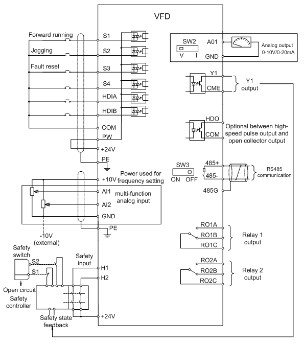
Figure 4–12 Wiring diagram of control circuit
Note: If wire-passing board outlet space is insufficient when all terminals on the control board are wired, cut the knock-out hole on the lower cover for wire outlet. If a dangerous situation occurs when the knock-out hole is cut for a purpose but not wire outlet, we will not bear any responsibility.
Terminal name | Instruction | |
+10V | The VFD provides +10.5V power | |
AI1 | 1. Input range: AI1 voltage/current can choose 0–10/ 0–20mA; AI2: -10V–+10V voltage; 2. Input impedance: 20kΩ during voltage input; 250Ω during current input; 3. AI1 voltage or current input is set by P05.50; 4. Resolution ratio: When 10V corresponds to 50Hz, the min. resolution ratio is 5mV; 5. 25°C, When input above 5V or 10mA, the error is ±0.5% | |
AI2 | ||
GND | +10.5V reference zero potential | |
AO1 | 1. Output range: 0–10V voltage or 0–20mA current 2. Voltage or current output is set by toggle switch SW2; 3. 25°C, when input above 5V or 10mA, the error is ±0.5%. | |
RO1A | RO1 relay output; RO1A is NO, RO1B is NC, RO1C is common port Contact capacity: 3A/AC250V, 1A/DC30V | |
RO1B | ||
RO1C | ||
RO2A | RO2 relay output; RO2A is NO, RO2B is NC, RO2C is common port Contact capacity: 3A/AC250V, 1A/DC30V | |
RO2B | ||
RO2C | ||
HDO | 1. Switch capacity: 50mA/30V; 2. Range of output frequency: 0–50kHz 3. Duty ratio: 50% | |
COM | Common port of +24V | |
CME | Common port of open collector output; short connected to COM by default | |
Y1 | 1. Switch capacity: 50mA/30V; 2. Range of output frequency: 0–1kHz | |
485+ | 485 communication port, 485 differential signal port and standard 485 communication interface should use twisted shielded pair; the 120ohm terminal matching resistor of 485 communication is connected by toggle switch SW3. | |
485- | ||
PE | Grounding terminal | |
PW | Provide input digital working power from external to internal; Voltage range: 12–30V | |
24V | The VFD provides user power; the max. output current is 200mA | |
COM | Common port of +24V | |
S1 | Digital input 1 | 1. Internal impedance: 3.3kΩ 2. Accept 12–30V voltage input 3. This terminal is bi-directional input terminal and supports NPN/PNP connection modes 4. Max. input frequency: 1kHz 5. All are programmable digital input terminals, users can set the terminal function via function codes |
S2 | Digital input 2 | |
S3 | Digital input 3 | |
S4 | Digital input 4 | |
HDIA | Besides S1–S4 functions, it can also act as high frequency pulse input channel Max. input frequency: 50kHz; Duty ratio: 30%–70%; Supports the input of a quadrature encoder with 24V power supply; equipped with speed-measurement function | |
HDIB | ||
+24V—H1 | STO input 1 | 1. Safe torque off (STO) redundant input, connect to external NC contact, STO acts when the contact opens, and the VFD stops output; 2. Safety input signal wires use shielded wire whose length is within 25m; 3. H1 and H2 terminals are short connected to +24V by default; it is required to remove the short-contact tag on the terminal before using STO function. |
+24V—H2 | STO input 2 | |
4.4.2 Input/output signal connection diagram
Set NPN /PNP mode and internal/external power via U-type short-contact tag. NPN internal mode is adopted by default.
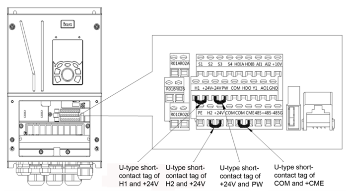
Figure 4–13 Position of U-type short-contact tag
If input signal comes from NPN transistors, set the U-type short-contact tag between +24V and PW based on the power used according to the figure below.
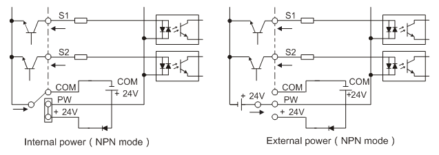
Figure 4–14 NPN mode
If input signal comes from PNP transistor, set the U-type short-contact tag based on the power used according to the figure below.
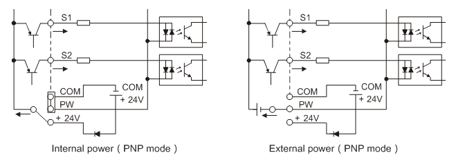
Figure 4–15 PNP mode