Function code | Name | Detailed instruction of parameters | Default value | Modify |
P05.00 | HDI input selection | 0: High pulse input. See P05.49–P05.54 1: Digital input. See P05.09. | 0 | ◎ |
P05.01 | S1 terminals function selection | 0: No function 1: Forward rotation operation 2: Reverse rotation operation 3: 3-wire control operation 4: Forward jogging 5: Reverse jogging 6: Coast to stop 7: Fault reset 8: Operation pause 9: External fault input 10: Increasing frequency setting(UP) 11: Decreasing frequency setting(DOWN) 12: Frequency setting clear 13: Shift between A setting and B setting 14: Shift between combination setting and A setting 15: Shift between combination setting and B setting 16: Multi-step speed terminal 1 17: Multi-step speed terminal 2 18: Multi-step speed terminal 3 19: Multi- step speed terminal 4 20: Multi- step speed pause 21: ACC/DEC time 1 22: ACC/DEC time 2 23: Simple PLC stop reset 24: Simple PLC pause 25: PID control pause 26: Traverse Pause (stop at the current frequency) 27: Traverse reset (return to the center frequency) 28: Counter reset 29: Torque control disabling 30: ACC/DEC disabling 31: Counter trigging 32: Length reset 33: Cancel the frequency change setting temporarily 34: DC brake 35: Shift the motor 1 into motor 2 36: Shift the command to the keypad 37: Shift the command to the terminals 38: Shift the command to the communication 39: Pre-magnetized command 40: Comsumption power clear 41: Comsumption power holding 42–60: Reserved 61: PID pole switching 62–63: Reserved | 1 | ◎ |
P05.02 | S2 terminals function selection | 4 | ◎ | |
P05.03 | S3 terminals function selection | 7 | ◎ | |
P05.04 | S4 terminals function selection | 0 | ◎ | |
P05.05 | S5 terminals function selection | 0 | ◎ | |
P05.06 | S6 terminals function selection | 0 | ◎ | |
P05.07 | S7 terminals function selection | 0 | ◎ | |
P05.08 | S8 terminals function selection | 0 | ◎ | |
P05.09 | HDI terminal function selection | 0 | ◎ | |
P05.10 | Polarity selection of the input terminals | The function code is used to set the polarity of the input terminals. Set the bit to 0, the input terminal is anode. Set the bit to 1, the input terminal is cathode.
Setting range: 0x000–0x1FF | 0x000 | ○ |
P05.11 | ON-OFF filter time | Set the sample filter time of S1–S8 and HDI terminals. If the interference is strong, increase the parameter to avoid the disoperation. 0.000–1.000s | 0.010s | ○ |
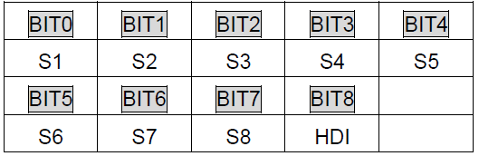
P05.12 | Virtual terminals setting | 0x000–0x1FF(0: Disabled, 1: Enabled) BIT0: S1 virtual terminal BIT1: S2 virtual terminal BIT2: S3 virtual terminal BIT3: S4 virtual terminal BIT4: S5 virtual terminal BIT5: S6 virtual terminal BIT6: S7 virtual terminal BIT7: S8 virtual terminal BIT8: HDI virtual terminal Note: After a virtual terminal is enabled, the state of the terminal can only be modified through communication, and the communication address is 0x200A. | 0x000 | ◎ |
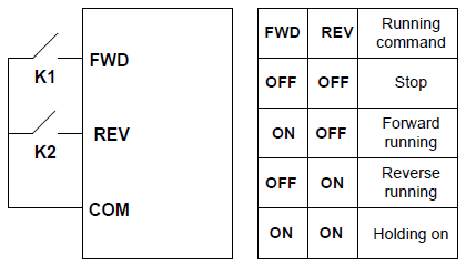
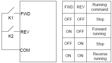
P05.13 | Terminals control running mode | Set the control operation mode of the terminals. 0: 2-wire control 1; the enabling function and direction determination function are integrated. This mode is widely used. It determines the rotation direction by the defined FWD and REV terminals command.
1: 2-wire control 2; the enabling function and the direction determination function are separated. In this mode, FWD is the enablingterminal, and the direction depends on the state of the defined REV.
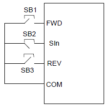
2: 3-wire control 1; in this mode, SIn is the enabling terminal, and the running command is generated by FWD and the direction is controlled by REV. SIn must be in the closed state when the VFD is running. The FWD terminal generates a rising edge signal, and the VFD starts to run. The status of the REV terminal determines the running direction. When the VFD stops, the SIn terminal needs to be disconnected to complete the stopping.
The direction control is as follows during operation:
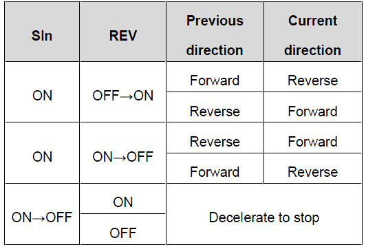
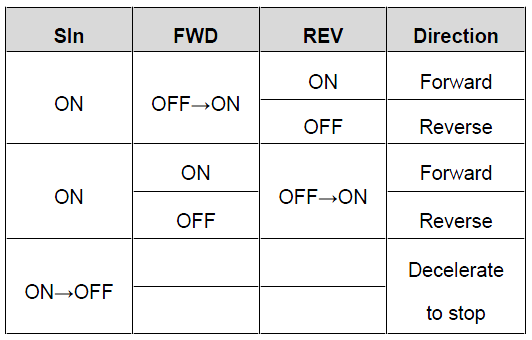
SIn: 3-wire control; FWD: Forward running; REV: Reverse running 3: 3-wire control mode 2. In this mode, SIn is defined as the enabling terminal, the running command is determined by the FWD or REV terminal, and the direction is determined by the FWD and REV terminals. When the VFD is running, terminal SIn must be in the connected state. Terminal FWD or REV generates a rising edge signal to run the VFD and determine its running direction. To stop the running of the VFD, you need to disconnect terminal SIn.
SlnFWDREVDirectionONOFF→ONONForwardOFFReverseONONOFF→ONForwardOFFReverseON→OFF Decelerate to stop SIn: 3-wire operation control; FWD: Forward running; REV: Reverse running Note:For the 2-wire running mode, when the FWD/REV terminal is valid, and the VFD stops because of the stop command from other sources, the VFD won't work when the stopping command is canceled even the control terminal FWD/REV is still valid;. Only when FWD/REV is re-triggered, the VFD can start again. For example, the PLC single-cycle stop command, fixed-period stop command, and the STOP/RST stop command that is valid in terminal control mode (see P07.04). | 0 | ◎ |
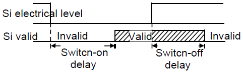
P05.14 | Switch-on delay of S1 terminal | The function code defines the corresponding delay time of electrical level of the programmable terminals during switching on and switching off.
Setting range: 0.000–50.000s | 0.000s | ○ |
P05.15 | Switch-off delay of S1 terminal | 0.000s | ○ | |
P05.16 | Switch-on delay of S2 terminal | 0.000s | ○ | |
P05.17 | Switch-off delay of S2 terminal | 0.000s | ○ | |
P05.18 | Switch-on delay of S3 terminal | 0.000s | ○ | |
P05.19 | Switch-off delay of S3 terminal | 0.000s | ○ | |
P05.20 | Switch-on delay of S4 terminal | 0.000s | ○ | |
P05.21 | Switch-off delay of S4 terminal | 0.000s | ○ | |
P05.22 | Switch-on delay of S5 terminal | 0.000s | ○ | |
P05.23 | Switch-off delay of S5 terminal | 0.000s | ○ | |
P05.24 | Switch-on delay of S6 terminal | 0.000s | ○ | |
P05.25 | Switch-off delay of S6 terminal | 0.000s | ○ | |
P05.26 | Switch-on delay of S7 terminal | 0.000s | ○ | |
P05.27 | Switch-off delay of S7 terminal | 0.000s | ○ | |
P05.28 | Switch-on delay of S8 terminal | 0.000s | ○ | |
P05.29 | Switch-off delay of S8 terminal | 0.000s | ○ | |
P05.30 | Switch-on delay of HDI terminal | 0.000s | ○ | |
P05.31 | Switch-off delay of HDI terminal | 0.000s | ○ | |
P05.32 | Lower limit of AI1 | The function code defines the relationship between the analog input voltage and its corresponding set value. If the analog input voltage beyond the set minimum or maximum input value, the VFD will count at the minimum or maximum one. When the analog input is the current input, the corresponding voltage of 0–20 mA is 0–10V. In different cases, the corresponding rated value of 100.0% is different. See the application for detailed information. The figure below illustrates different applications:
Input filter time: this parameter is used to adjust the sensitivity of the analog input. Increasing the value properly can enhance the anti-interference of the analog, but weaken the sensitivity of the analog input. Note: Analog AI1 and AI2 can support 0–10V or 0–20mA input, when AI1 and AI2 selects 0–20mA input, the corresponding voltage of 20mA is 5V. AI3 can support the output of -10V–+10V. Setting range of P05.32: 0.00V–P05.34 Setting range of P05.33: -100.0%–100.0% Setting range of P05.34: P05.32–10.00V Setting range of P05.35: -100.0%–100.0% Setting range of P05.36: 0.000s–10.000s Setting range of P05.37: 0.00V–P05.39 Setting range of P05.38: -100.0%–100.0% Setting range of P05.39: P05.37–10.00V Setting range of P05.40: -100.0%–100.0% Setting range of P05.41: 0.000s–10.000s Setting range of P05.42: -10.00V–P05.44 Setting range of P05.43: -100.0%–100.0% Setting range of P05.44: P05.42–P05.46 Setting range of P05.45: -100.0%–100.0% Setting range of P05.46: P05.44–10.00V Setting range of P05.47: -100.0%–100.0% Setting range of P05.48: 0.000s–10.000s | 0.00V | ○ |
P05.33 | Corresponding setting of the lower limit of AI1 | 0.0% | ○ | |
P05.34 | Upper limit of AI1 | 10.00V | ○ | |
P05.35 | Corresponding setting of the upper limit of AI1 | 100.0% | ○ | |
P05.36 | AI1 input filter time | 0.100s | ○ | |
P05.37 | Lower limit of AI2 | 0.00V | ○ | |
P05.38 | Corresponding setting of the lower limit of AI2 | 0.0% | ○ | |
P05.39 | Upper limit of AI2 | 10.00V | ○ | |
P05.40 | Corresponding setting of the upper limit of AI2 | 100.0% | ○ | |
P05.41 | AI2 input filter time | 0.100s | ○ | |
P05.42 | Lower limit of AI3 | -10.00V | ○ | |
P05.43 | Corresponding setting of the lower limit of AI3 | -100.0% | ○ | |
P05.44 | Middle value of AI3 | 0.00V | ○ | |
P05.45 | Corresponding middle setting of AI3 | 0.0% | ○ | |
P05.46 | Upper limit of AI3 | 10.00V | ○ | |
P05.47 | Corresponding setting of the upper limit of AI3 | 100.0% | ○ | |
P05.48 | AI3 input filter time | 0.100s | ○ | |
P05.49 | HDI high-speed pulse input function selection | The function selection when HDI terminals is high-speed pulse input 0: Frequency setting input, frequency setting source 1: Counter input, high-speed pulse counter input terminals 2: Length counting input, length counter input terminals | 0 | ◎ |
P05.50 | Lower limit frequency of HDI | 0.000kHz–P05.52 | 0.000 kHz | ○ |
P05.51 | Corresponding setting of HDI low frequency setting | -100.0%–100.0% | 0.0% | ○ |
P05.52 | Upper limit frequency of HDI | P05.50–50.000kHz | 50.000 kHz | ○ |
P05.53 | Corresponding setting of upper limit frequency of HDI | -100.0%–100.0% | 100.0% | ○ |
P05.54 | HDI frequency input filter time | 0.000s–10.000s | 0.010s | ○ |