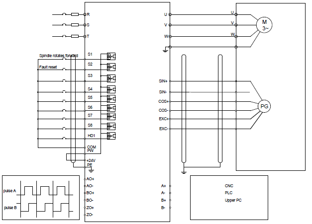
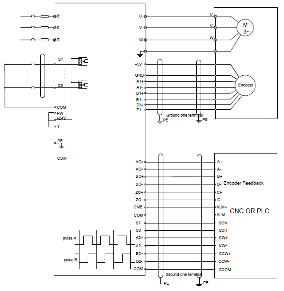
4.4.1 Wiring diagram of basic control circuit
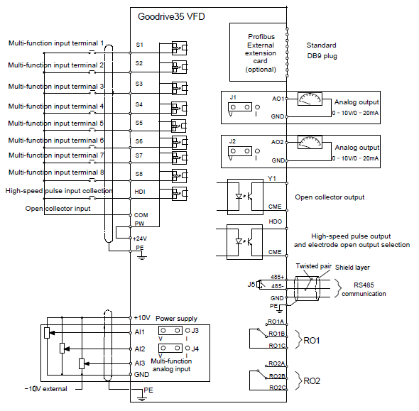
Figure 4‑20 Wiring of control circuit
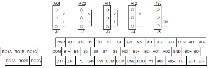
Terminalname | Description | ||||
+10V | Local power supply +10 V | ||||
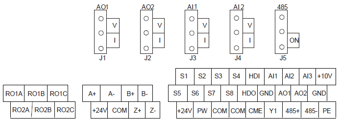
AI1 | 1. Input range: AI1/AI2 voltage and current can be chosen: 0–10 V/0–20mA; AI1 can be shifted by J3 while AI2 can be shifted by J4; AI3: -10 V–+10 V 2. Input impedance: voltage input: 20kΩ; current input: 500Ω 3. Resolution: the minimum one is 5m V when 10 V corresponds to 50 Hz 4. Deviation ±1%, 25°C | ||||
AI2 | |||||
AI3 | |||||
GND | +10 V reference null potential | ||||
AO1 | 1. Output range: 0–10 V or -20–20mA; The voltage or the current output is depended on the jumper. AO1 is switched by J1 and AO2 is switched by J2 2. Deviation±1%, 25°C | ||||
AO2 | |||||
Terminalname | Description | |||
RO1A | RO1 relay output; RO1A is NO, RO1B is NC, RO1C is common port Contact capacity: 3A/AC250V, 1A/DC30V | |||
RO1B | ||||
RO1C | ||||
RO2A | RO2 relay output; RO2A is NO, RO2B is NC, RO2C is common port Contact capacity: 3A/AC250V, 1A/DC30V | |||
RO2B | ||||
RO2C | ||||
Terminalname | Description | |||
HDO | 1. Switch capacity: 200mA/30V; 2. Range of output frequency: 0–50kHz | |||
COM | Common port of +24V | |||
CME | Common port of open collector output | |||
Y | 1. Switch capacity: 200mA/30V; 2. Range of output frequency: 0–1kHz | |||
485+ | For 485 communication port, 485 differential signal port and standard 485 communication interfaces, use twisted pairs or shielded cables. | |||
485- | ||||
Terminalname | Description | |||||||
PE | Grounding terminal | |||||||
PW | Provide input digital working power from external to internal; Voltage range: 12–30V | |||||||
24V | The VFD provides user power; the maximum output current is 200mA | |||||||
COM | Common port of +24V | |||||||
S1 | Digital input 1 | 1. Internal impedance: 3.3kΩ 2. Accept 12–30V voltage input 3. This terminal is bi-directional input terminal and supports NPN/PNP connection modes 4. Max. input frequency: 1kHz 5. All are programmable digital input terminals, and users can set the terminal function via function codes | ||||||
S2 | Digital input 2 | |||||||
S3 | Digital input 3 | |||||||
S4 | Digital input 4 | |||||||
S5 | Digital input 5 | |||||||
S6 | Digital input 6 | |||||||
S7 | Digital input 7 | |||||||
S8 | Digital input 8 | |||||||
HDI | Besides S1–S8 functions, it can also act as high frequency pulse input channel Max. input frequency: 50kHz | |||||||
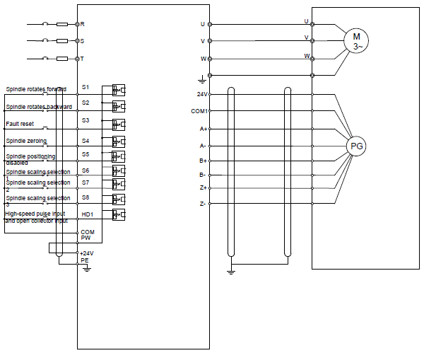
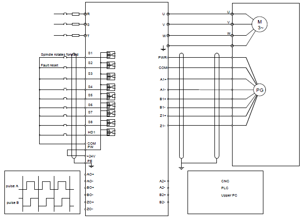
4.4.2 C1 terminal (EC-PG301-24) instruction and the wiring diagram
4.4.2.2 Terminal instruction
Terminal name | Instruction |
+24 V | Encoder power supply. It can provide power supply of 24 V, 200 mA. |
A+, A-, B+, B-, Z+, Z- | Support encoder signal differential, push-pull, and open collector input. |
COM1 | Power supply ground of the encoder |
Note: Refer to section 4.4.1 for detailed information of AO1, AO2, AI1, AI2, 485 and other terminals.
4.4.2.3 Wiring diagram
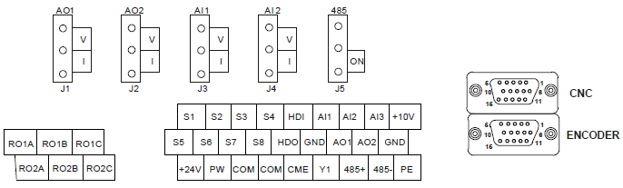
4.4.3 D1 terminal (EC-PG304-05) instruction and the wiring diagram
4.4.3.1 Terminal arrangement
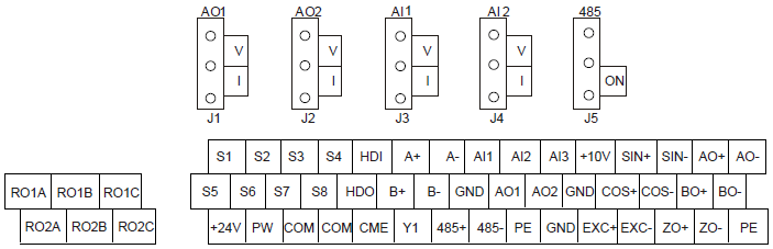
4.4.3.2 Terminal instruction
Terminal name | Instruction |
EXC+EXC- | Exciting signal of 10k Hz, and max. output current of 100 mA. |
SIN+, SIN- , COS+ and COS- | Encoder differential signal input. |
A+, A-, B+, B- | Pulse reference signal, default as 5 V input. External current-limiting resistor is needed when the input voltage is above 10 V. |
AO+, AO-, BO+, BO-, ZO+, ZO- | Frequency-divided output of encoder signals, 5 V differential signals Frequency dividing ratio: 1:1 |
Note: Refer to section 4.4.1 for detailed information of AO1, AO2, AI1, AI2, 485 and other terminals.
4.4.3.3 Wiring diagram
4.4.4 H1 terminal (EC-PG305-12) instruction and the wiring diagram
Terminal name | Instruction |
PWR | Power supply, provide 5 V/12 V, 200mA power supply |
A1+, A1-, B1+, B1-, Z1+, Z1- | Encoder differential, open collector, and push-pull signal input |
A2+, A2-, B2+, B2-, | Support encoder differential, open collector, and push-pull pulse reference signal. Pulse reference signal, default as 5 V input. External current-limiting resistor is needed when the input voltage is above 10 V |
AO+, AO-, BO+, BO-, ZO+ and ZO- | Frequency-divided output of encoder pulse signals, 5 V differential signals Frequency dividing ratio: 1:1 |
COM | Power supply ground of the encoder |
Note: Refer to section 4.4.1 for detailed information of AO1, AO2, AI1, AI2, 485 and other terminals.
4.4.4.3 Wiring diagram
4.4.5 H2 terminal (EC-PG305-05) instruction and the wiring diagram
4.4.5.2 Interfaces instruction
DB15 (CNC) | CNC system interface signal | DB15 (ENCODER) | Encoder interface signal |
1 | AO+ | 1 | +5 V |
2 | AO- | 2 | A1+ |
3 | BO+ | 3 | B1+ |
4 | BO- | 4 | Z1+ |
5 | ZO+ | 5 | U+ |
6 | ZO- | 6 | U- |
7 | CME | 7 | V+ |
8 | COM | 8 | V- |
9 | S7 | 9 | GND |
10 | S8 | 10 | A1- |
11 | A2+ | 11 | B1- |
12 | A2- | 12 | Z1- |
13 | B2+ | 13 | W+ |
14 | B2- | 14 | W- |
15 | COM | 15 |
Terminal name (CNC) | Instruction |
A2+, A2-, B2+, B2- | 5 V differential pulse + direction reference signal, Support 400 kHz at maximum |
AO+, AO-, BO+, BO-, ZO+, ZO- | Frequency-divided output of encoder pulse signals, 5 V differential signals Frequency dividing ratio: 1:1 |
CME, COM | Alarm output (If use this function, it is necessary to short-connect Y terminal to +24 V terminal, and remove the tag between CME and COM terminal) |
Terminal name (ENCODER) | Instruction |
S7 | Common digital input |
+5 V, GND | Encoder power supply, support 5 V±5%, 200mA power |
A1+, A1-, B1+, B1-, Z1+, Z1- | The encoder differential input signal, support 400 kHz at maximum |
U+, U-, V+, V-, W+, W- | Difference angle input signal input of UVW encoders (not for incremental encoders) |
Note: Refer to section 4.4.1 for detailed information of AO1, AO2, AI1, AI2, 485 and other terminals.
4.4.5.4 The wiring diagram
4.4.6 S1 terminal (EC-PG302-05) instruction
4.4.6.1 Sin/cos terminal layout
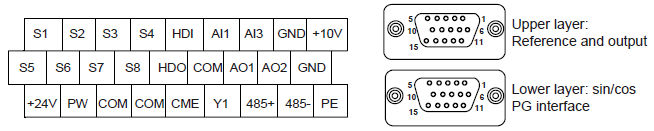
4.4.6.2 DB15 interface instruction
DB15 (upper layer) | Pulse reference and output interface signal | DB15 (Lower layer) | Sin/cos encoder interface signal |
1 | AO+ | 1 | B- |
2 | AO- | 2 | Null |
3 | BO+ | 3 | R+ |
4 | BO- | 4 | R- |
5 | ZO+ | 5 | A+ |
6 | ZO- | 6 | A- |
7 | / | 7 | 0 V |
8 | / | 8 | B+ |
9 | / | 9 | 5 V |
10 | / | 10 | C- |
11 | A2+ | 11 | C+ |
12 | A2- | 12 | D+ |
13 | B2+ | 13 | D- |
14 | B2- | 14 | Null |
15 | / | 15 | Null |
4.4.6.3 DB15 pin function instruction
Name of upper layer terminal (pulse reference interface) | Instruction |
A2+, A2-, B2+, B2-, | 5 V differential quadrature pulse reference signal, support 400 kHz at maximum |
AO+, AO-, BO+, BO-, ZO+, ZO- | Frequency-divided output of encoder pulse signals, 5 V differential signals Frequency dividing ratio: 1:1 |
Name of lower layer terminal (sin/cos encoder interface) | Instruction |
+5 V, 0 V | Encoder power, can provide 5 V±5%, 200mA. |
A+, A-, B+, B-, C+, C-, D+, D-, R+, R- | Sin/cos encoder signal input, support SINA/SINB/SINC/SIND 0.8–1.2 Vpp, SINR 0.2–0.85 Vpp, 200 kHz at maximum |
4.4.7 Input/output signal connection diagram
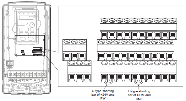
Figure 4‑21 U-shaped contact tag
If the signal is from NPN transistor, please set the U-shaped contact tag between +24 V and PW as below according to the used power supply.
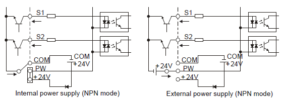
Figure 4‑22 NPN modes
If the signal is from PNP transistor, please set the U-shaped contact tag as below according to the used power supply.
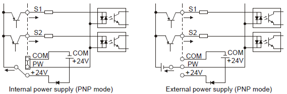
Figure 4‑23 PNP modes